Dual MMIC Amplifier
for 1 to 4 GHz
This project was conceived to provide a tried &
tested amplifier for both my amateur radio projects and also to give to
students as a basic building block to drive RF power devices to around about
the 1 watt level ( from the tracking generators in the Spectrum & Vector
Network Analysers ) for either Wlan or Wimax power amplifier projects. It was
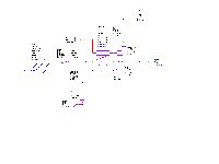
designed to be as flexible in nature so is two stages of SOT89 or MP86 package
MMIC's with provision for attenuators to set the overall stage gain / allow
some protection of the MMIC's in a research & teaching lab environment.
Both Minicircuits
& Hittite have
a range of suitable MMIC amplifiers , the student just has to choose the
suitable combination for Frequency response , Power output & Gain
required for their project , the attenuators are made up using "
Preferred Value " resistors so their attenuation is not " Whole dB's
" the 1dB attenuator on the output ensures the following stage "
see's a resistive source at all frequencies ", the use of twin resistors
for the shunt element's improves the return loss of the attenuator as well as
increasing the power dissipation at that point in the circuit.The circuit is
modelled as usual using Microwave Office
from AWR , but could just as easily be modelled using the
Ansoft
Designer SV package which is currently free or any other suitable RF
modeling package.The circuit uses an attenuator on the input to ensure
stability given the high gain of the MMIC and also to provide a resistive load
to any preceding stage eg filter . The stages will be fed from a small voltage
regulator to ensure the gain remains stable in a lab environment ( people
rarely set bench top power supplies to the same value each time they use them )
the amplifier module was designed to fit in a standard commercial tinplate case
measuring 50 x 25 x15 mm using a pair of SMA sockets for input / output
connections with the upper & lower groundplanes soldered to the case to
provide a low inductance grounding , the earth planes nearer to the
microstriplines were " Tied " together using my traditional technique
of 0.5 mm holes with a single strand of 0.2 mm wire from ordinary instrument
wire to suck the solder in by capillary action , the same is applied to the
grounding of the tabs on the MMIC's to ensure a low thermal path as well as
good RF earthing. The circuit was laid out with Microwave Office using the component libraries
for ALL the parts as listed in the various supplier's catalogues
to ensure that the parts chosen were freely available ( Preferably from more
than one supplier ) with the full manufacturer's part no. checked in the
Microwave Office Online component libraries
or downloaded from the manufacturer's own websites , as a result of laying out
the circuit with all the relevant tracks junctions & components it's quite
easy to see ALL the circuit elements involved in making just a simple two stage
amplifier ( It fills an A3 page ), the Voltage regulator circuit was added
later in the CAD layout of the board after it had been generated in
Microwave Office using the
relevant layout tools this means that you can see the effects of the grounding
you add as you create a full PCB artwork rmembering to ADD all the relevant
text to aid testing & inspection of the completed project. Having created
the schematic in the modelling package the design is then transferred to a
basic layout this only has components microstrip on it the ground plane and
board outline together with the relevant text to be etched on the Top copper
layer are now added , this enables you to check that any grounding alongside
microstripline does not turn into " Coplanar stripline " shold you
need to extend tracks up to the edge of the board to fit it in a standard box
then these can easily be re - modelled at this stage before committing the
design to production . The stages in reaching the completed
artwork ( including the " Mirroring " to produce a contact print )
are detailed in the modelling package but the instructions are often buried
several layers down in the help files . This is a simple stage by stage set of
instructions to enable anybody starting off using the modelling packages to get
an artwork out ready for exposing a Photo - Sensitve PCB substrate . The case
is actually made by using two lids & one body from the standard "
Solder in " range as the specific case size is not available although
larger versions of the case are available in the correct style .
The simple " Step by Step " instructions
for using Microwave Office for this project are
listed below
Lay out your circuit using the relevant components &
symbols from the library .
Then add all the graphs you think you will need together
with any text, when you have your desired amplifier completed at schematic
level .
Then convert it to a layout using the relevant part of
the program , you will end up with a " Rat's Nest " of all the parts
.
Now lay these out as per your circuit diagram , the
individual elements in the layout are highlighted as you move them ( if you
wish to check back to the schematic you will see them highlighted accordingly
in Green ).
Then add a shape for the housing you intend using using
the " Layout
editor " ( Toolbar at the bottom of the screen or drop
down menu ) to " Add
Shape " this will put a shape up coloured in as
" Error " initially .
Then by using the "
Shape Properties " command you
can change it to " Board
Outline ", then you can repeat the " Add shape
" routine to ADD the groundplane as you require
" Copper Layer
" being chosen . By returning to the schematic part of the program
you can see the effects on the circuit of adding the grounding areas changing
line lengths to fit the board outline etc , Text can be added using the text
editor on the taskbar ( The same way as you added text to you circuit &
graphs earlier ).
Then when you have your completed design laid out copy
the whole layout & mirror it and place it on the page below the "
Normal " layout , you are now ready to export your completed layout in to
one of the CAD packages mentioned on this website , exporting it as a
" Flat DXF
" is the easiest option , this is then read in to the CAD package (
You will have to set the drawing defaults up at this stage see the
relevant webpage
) .
Then you can finally colour the relevant areas of you
layout in according to whether you require a photo positive or photo negative
artwork you will need to choose the approriate colours for all the lines in the
drawing otherwise the individual shapes drawn will be just that NOT joined up
tracks !
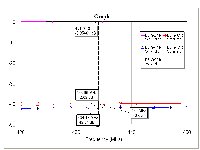
The Circuit design and Graph of modelled results
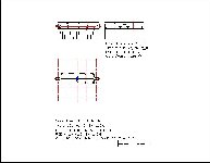
The PCB Layouts are shown in stages ,the only
difference between the artworks is the ground has been added using the Layout
editor in MWO for the second PCB layout and the
mirrored artwork has been added in the second layout.
The CAD artwork this is derived from second layout above
, the DXF exported from MWO with the normal &
mirrored layouts ready to fill to create the " Contact " print which
can also be copied in to a word document .
Alternative value attenuators for gain setting
Circuit of the Attenuators
Graphs of Attenuation & Return Loss ( 1, 2, 3 &
5dB )
Graphs of Attenuation & Return Loss ( 6 ,10 dB
)
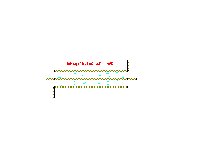
The Finished module

Parts Listing for the Module ( Includes all gain setting
values )
| Item |
Manufacturer |
Part No. |
Supplier |
Supplier's Part No
|
QTY |
| 78M08 |
Various |
78M08ACDT |
Farnell
|
516 - 4929 |
1 |
| GALI5 |
Minicircuits
|
GALI - 5 |
Minicircuits
|
GALI - 5+
|
1 |
| GVA84 |
Minicircuits |
GVA-84 |
Minicircuits |
GVA - 84+
|
1 |
| 1R2 " 0603
" |
Various |
|
Various
|
|
2 |
| 5R6 " 0603
" |
Various |
|
Various |
|
1 |
| 12R " 0603
" |
Various
|
|
Various
|
|
1 |
| 18R " 0603
" |
Various
|
|
Various
|
|
1 |
| 33R " 0603
" |
Various
|
|
Various
|
|
1 |
| 39R " 0603
" |
Various
|
|
Various
|
|
1 |
| 180R " 0603
" |
Various
|
|
Various
|
|
4 |
| 330R " 0603
" |
Various
|
|
Various
|
|
4 |
| 390R " 0603
" |
Various
|
|
Various
|
|
4 |
| 680R " 0603
" |
Various
|
|
Various
|
|
4 |
| 820R " 0603
" |
Various
|
|
Various
|
|
4 |
| 1K8 " 0603
" |
Various
|
|
Various
|
|
4 |
| 100pF " 0603 " |
Various
|
|
Various
|
|
6 |
| 1nF " 0603
" |
Various
|
|
Various
|
|
2 |
| 100nF " 0603
" |
Various
|
|
Various
|
|
3 |
| SMA Socket |
Various
|
|
Farnell |
105 - 6374 |
2 |
| 10nH |
Coilcraft
|
1606 - 9 - LB
|
Coilcraft
|
1606 - 9 - LB
|
2 |
| 50 x 25 x 15
case |
Perancea |
PFL - 2 - T |
Farnell
|
118 - 1374 |
2 |
Back To Amateur Radio Projects
This page last updated 24/03/10
