
This is used to provide the correct level of drive to the main RF amplifier module as well as guaranteeing that the amplifier sees resistive source at all times .
The attenuator is a " Pi " type using surface mount resistors paralleled to get the correct value & power disspation 1 watt " 2512 " being used for the shunt elements and the series element the tracks being 50R micro - stripline chosen by using the correct dielectric material for the PCB substrate . The attenuator PCB is heatsinked to the case by using a small amount of heatsink paste under the board , the whole module is secured to the chassis to improve the heat dissipation when used for long periods of transmission using FM , for SSB use it required no additional heatsinking other than the case .
Internal view of the completed attenuator module
CAD Drawings for the Attenuator
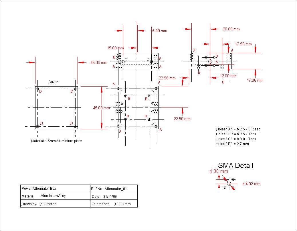
CAD drawing for the Attenuator housing
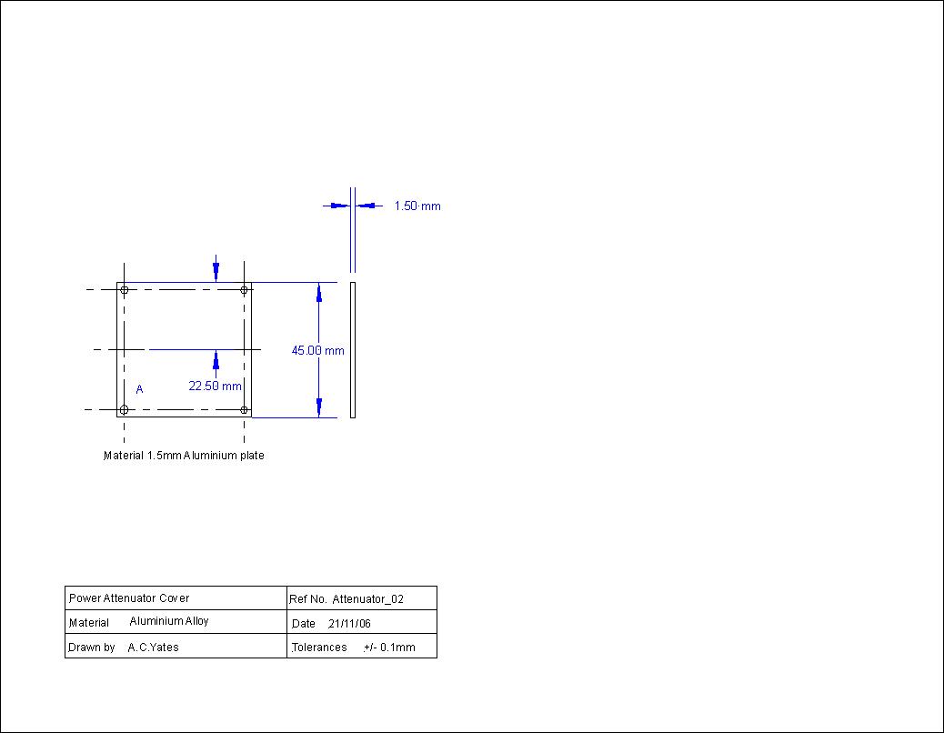
CAD Drawing for the Attenuator cover
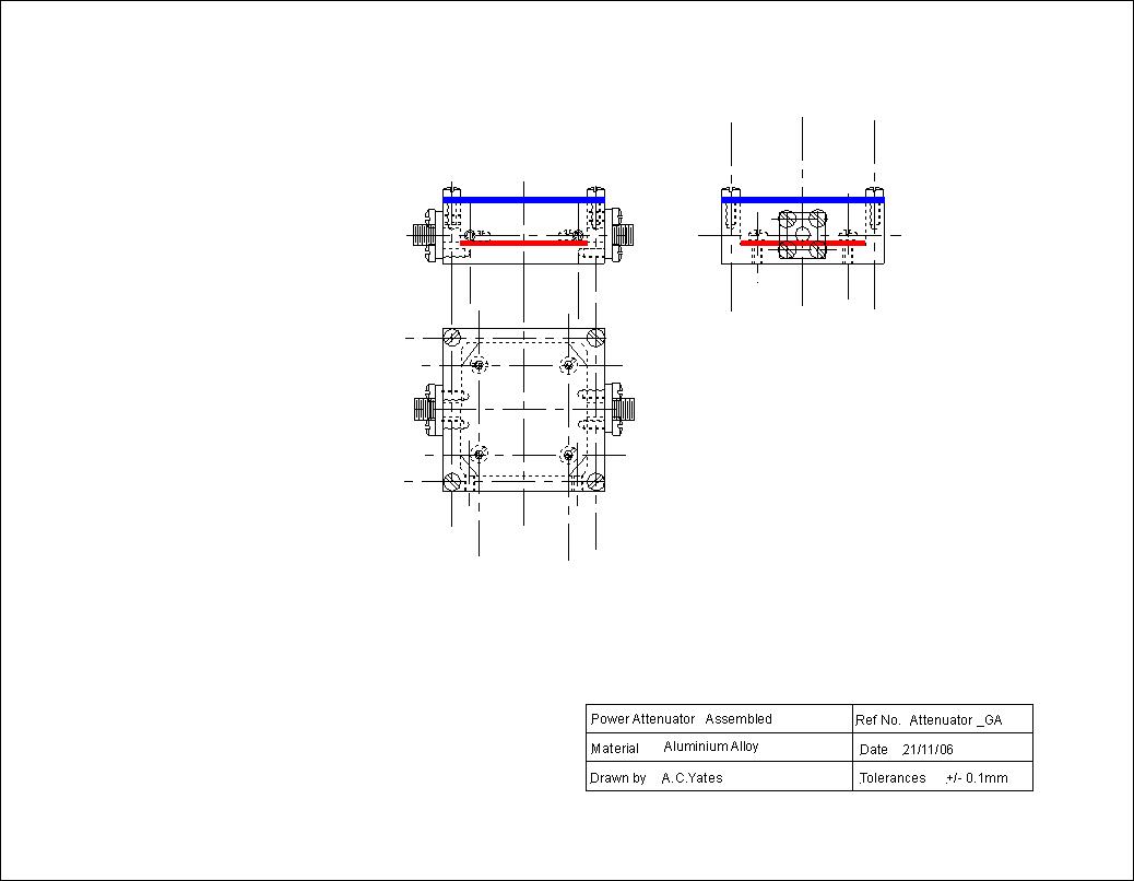
CAD Drawing of the Attenuator General Assembly
CAD artwork for the Attenuator ( Mirrored )
Parts listing for the Attenuator
| Item | Manufacturer | Part No. | Supplier | Supplier's Part No | QTY |
| Module housing | Home made | 1 | |||
| Module cover | Home made | 1 | |||
| 560R " 2512" | Various | RS | 228 - 0373 | 8 | |
| 39R "2512" | Various | FEC | 126 - 5201 | 1 | |
| SMA Socket | Various | FEC | 105 - 6376 | 2 | |
| M2.5 x 6 mm | Various | FEC | 142 - 0030 | 16 | |
| M2.5 crinkle washer | Various | FEC | 161 - 4000 | 4 | |
| M3 x 6 mm | Various | FEC | 142 - 0032 | 2 | |
| M3 crinkle washer | Various | FEC | 161 - 4001 | 2 | |
| Supplier codes | RS is RS Components | FEC is Farnell Electronic Components | |||
The assembled attenuator PCB was fitted into the module housing with a small amount of heatsink paste under the PCB to aid heat transfer and fixed down using the 4 off M2.5 screws , the SMA input & output connectors were then fitted & soldered to the PCB ready for testing .
Testing of the Input Attenuator
Testing of the attenuator was done initially using a network analyser to measure both S11 , S22 ( Input & Output Return loss ) & S21 ( Attenuation ) at low power as was done for the low pass filter then the unit was tested with the nominal 10 watt source & power attenuator / milliwatt power meter to check it's attenuation over about 10 minutes along with a thermometer to measure it's temperature rise . The nominal attenuation was designed to be 6dB but the actual value came out as 6.3dB when allowing for the use of " Preferred Value " resistors . The value of the attenuator was also noticed to have varied dependant on the temperature it reached, when above 40 deg C the value went up by 0.2dB to 6.5 dB , returning to 6.3 dB at ambient temperature ( 20 - 25 deg C )
This page last updated 27th Oct 2009