Circuit Modelling Design Notes for use with Modelling
Software
( Microwave Office and other Modelling
Packages )
When designing with a modelling package it is advisable
that when using " Discrete " components where ever possible to use
the so called " Prefered Values " , if the design value of a
capacitor is " non standard " then the use of multiple values to
arrive at the design value is a reasonable route to take, however try to avoid
using parts with too dissimilar a value .
The choice of package size also affects the performance
of your design so reference to full manufacturer's data sheet / S parameters is
advisable , try to choose the size of component to minimise any discontinuities
in circuit paths , eg if your transmission line is 2mm wide DO
NOT use a " 1206 " package device in it , its "3 .175 " mm wide ! use an
" 0805" . When you use a shunt component
from a transmission line to earth it is advisable to model the component coming
from a junction to allow you to get the correct length of transmission line the
junction size being equal to the package width of the shunt element , this also
allows for the discrete width of the components end cap to appear to be
distributed along the transmission line not just at a point as is the case in
the real circuit .This means that when you are optimising the track lengths
using the inbuilt tools , the capacitor / inductor is simply slid up / down the
transmission line as in real life .When using a capacitor in the transmission
line as a DC block try using a value that is series resonant you will be
suprised at the improvement in power transfer , this also applies when you are
decoupling a supply rail as it is more effective than just increasing the value
as you would think from 1st principles , with decoupling you may have to use
several values about a decade apart to ensure the supply is decoupled at
ALL frequencies where the active device has gain .
The following part will detail the design &
construction of a " Low Noise Amplifier for 1.8 - 2 Ghz " based on
the application note for the Avago ( Agilent / HP ) for the ATF54143 .
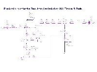
From the various ways in which the circuit is drawn you
can see the Significant change in results , the discrete components used
DO NOT CHANGE only the interconnections / physical spacing
.
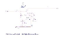
The initial circuit as copied from the application note
& drawn as a conventional circuit ( Schematic ) the interconnections in
Red have NO physical length nor do they have any losses THEY ARE
PERFECT !. The second circuit as
redrawn to include pads & transmission lines that are neccesary to make the
real amplifier including the relevant subcircuits from the package library or
the manufacturers website . This shows the benefit of using the relevant data
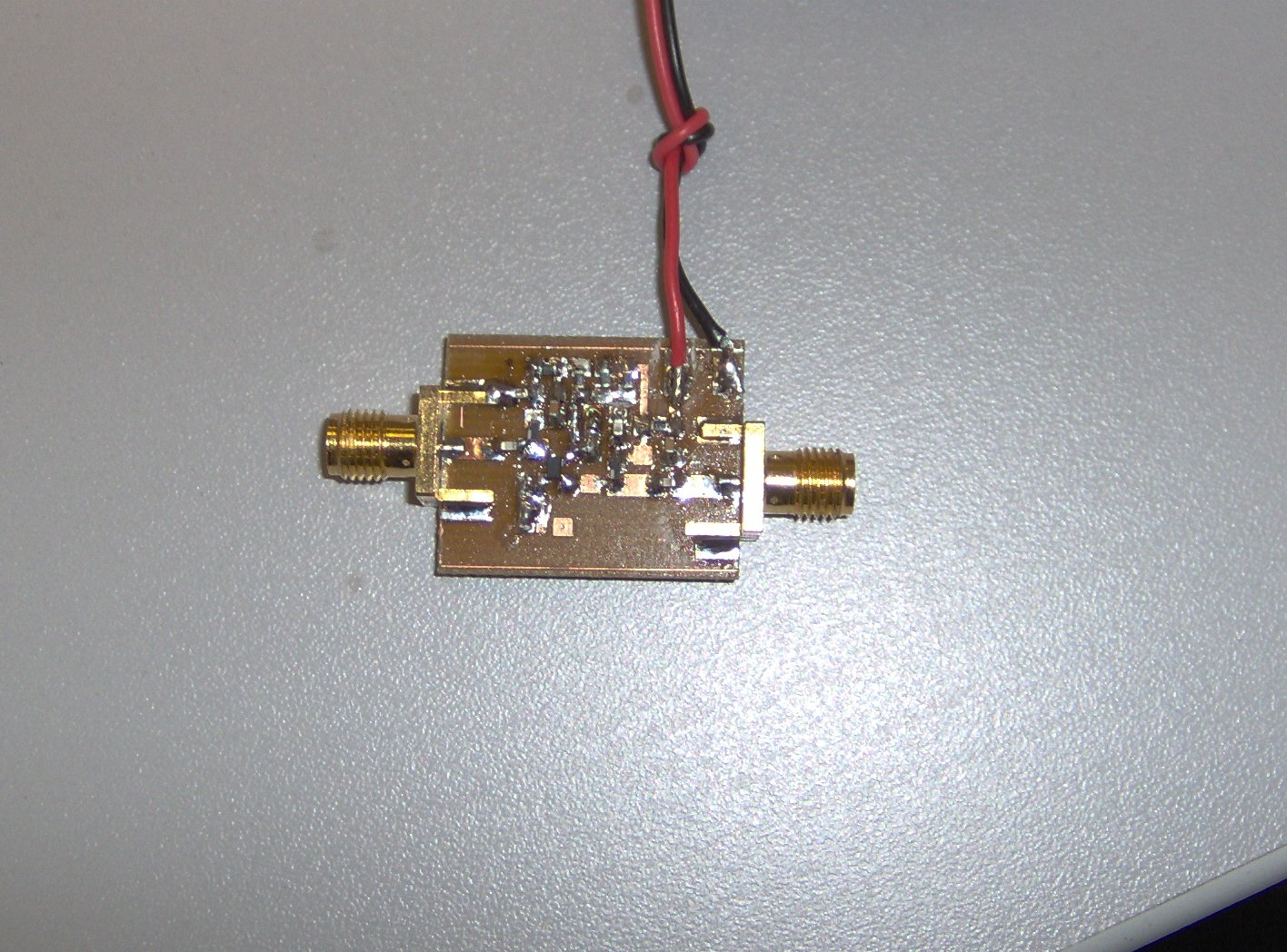
as the actual design was used on the " ACE Active Integrated Antennas
" Course held at the University of Birmingham in September 2008 .The
calculated gain was 16dB , the measured gain of the prototype being 15.7 dB ,
the course members who were all new to designing & building SMD RF
amplifiers managed to get gains of between 14.5 & 15.6 dB gain ( A Sample
of 10 items ) the variation being due to the placement of the degenerative
feedback links in the source path . The individual components were selected
from the online libraries ( Having checked the supplier's websites for full
component part No's ) the relevant layout was taken from the manufacturer's
application note .The necked in transmission line was created to allow for the
use of additional components on the original application note layout with the
narrow track being removed to allow for the addition of an inductor or resistor
( or both ) should the preamplifier be designed to work at the lower end of the
devices range ( It covers 100MHz - 6 GHz ) the gain being higher at lower
frequencies could lead to stability problems hence the provision in the board
layout to add these additional components.
The drawing above shows the way in which many people
would draw an amplifier from first principles for low frequencies , however
with a little thought you will realise that this is not what you can build in
real life the tracks between components DO have a finite length & width
!
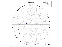
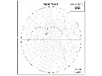
The input match of the idealised amplifier is not
matched to the system impedance as can be seen from the polar plot above
.
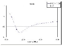
The same input match as shown on a
Return Loss plot , note the match is < 10dB flat above 2 GHz
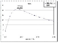
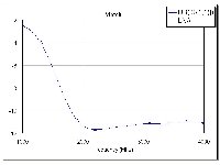
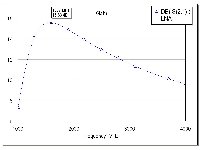
The Gain plot of the Idealised amplifier
using the component values from the Manufacturer's data sheet with the maximum
gain shown as 14.27 dB at 1725MHz.
Note the same component
values are used in this " Real " amplifier just the
realisitic application of Microstripline tracks & junctions in accordance
with the layout copied from the manufacturer's data sheet , see how the
matching , gain & frequency response have ALL been altered , just by the
ADDITION of real interconnections
The input match is certainly not perfect at the desired
frequency
The input Return Loss does show an improvement in as
much as there is a dip showing a limited amount of selectivity at the desired
frequency
Note the Significant change in the maximum gain value
& the frequency at which the maximum gain occurs !
The Values of gain & return loss will be altered by
the amount of degenerative feedback present in the source of the active device
,these in turn will also adjust the frequency slightly at which maximum stable
gain and best input & output match occur this can be seen when using the
" Tune " facility in Microwave office viewing the interaction between
all these on their relevant graphs .This can be seen more readily by putting
all four " S2P " graphs on a single plot and by putting both input
& output polar responses on a single plot .
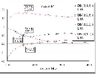
Graph of S11 , S12 , S21 & S22
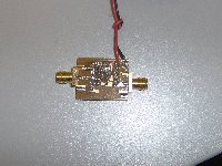
Picture of the " Real "
Amplifier
In addition to the design for the Gasfet amplifier shown
above there is a more detailed design for a two stage wideband MMIC amplifier
along with some other basic projects on this
Link
Back To RF Design Notes
This page last updated 2nd Sept 2010