Simple Microwave Office
Projects
These projects are aimed to give the novice an idea on
how to lay out various simple type of circuit , the design criteria for your
project will have already been decided for you , these projects are designed to
show you the various PRACTICAL implementations of your project from the basic
circuit which you would have used for lower frequency work ( as part of your
course ) both for passive & active designs .
Simple Band pass filter for
7.5 GHz using Microstriplines
This project illustrates the use of transmission lines
of variable widths being combined to produce a band pass filter this was used
in a forward scatter radar transmitter by the MISL group . It also high lights
the need for accurate modelling of ALL the relevant components , the
differences between the two circuit's responses highlights the need to be fully
aware of even the simplest of designs, the only difference being the addition
of step transitions between the capacitive & inductive striplines , the
lengths & widths of the actual striplines being the same in BOTH circuits ,
designing without these transitions results in a center frequency error of
about 10% , this was born out by constructing the filter with the step
transitions missing then testing it on a Network analyser , and comparing the
real world design with both modelled results ! The use of the step transition
is advisable when there is more than about a 25% variation in the width of
adjoining striplines .
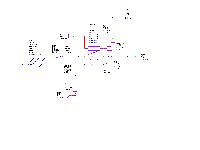
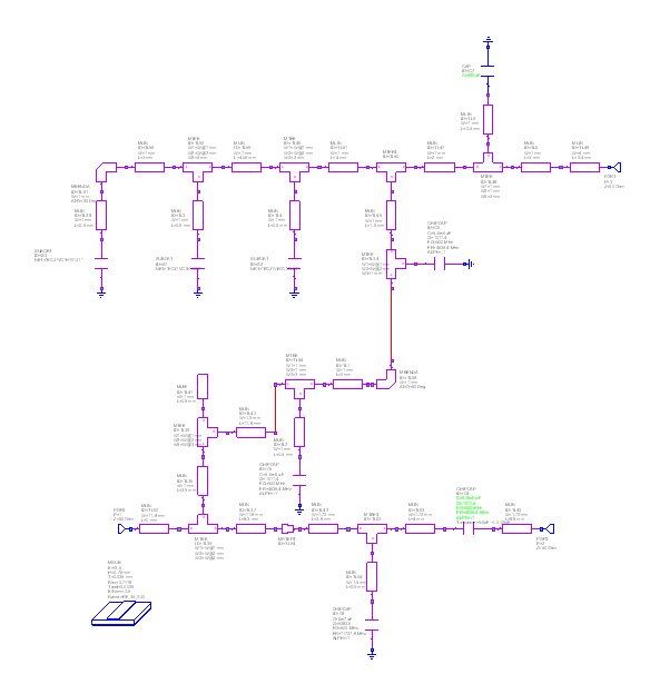
Basic MWO circuit (
microstrip elements )
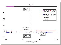
S11 , S21 Responses for
the MWO Basic circuit
Revised MWO circuit (
with simple microstrip & junctions)
S11 , S21 Responses for
the revised circuit
Comparison of Basic &
Revised circuits
MWO Artwork for the
Revised filter
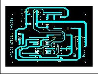
CAD generated
Artwork ( Photo - negative )
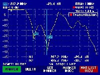
VNA Plot of real
filter
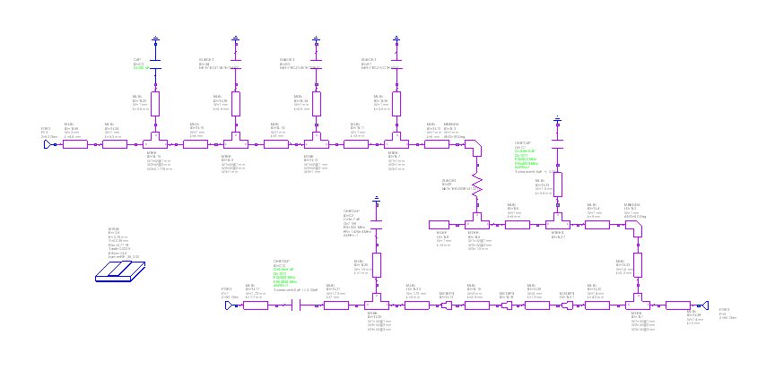
Dual MMIC Amplifier for 1 to 4
GHz
This project was conceived to provide a tried &
tested amplifier for both my amateur radio projects and also to give to
students as a basic building block to drive RF power devices to around about
the 1 watt level ( from the tracking generators in the Spectrum & Vector
Network Analysers ) for either Wlan or Wimax power amplifier projects. It was
designed to be as flexible in nature so is two stages of SOT89 or MP86 package
MMIC's with provision for attenuators to set the overall stage gain / allow
some protection of the MMIC's in a research & teaching lab environment.
Both Minicircuits
& Hittite have
a range of suitable MMIC amplifiers , the student just has to choose the
suitable combination for Frequency response , Power output & Gain
required for their project , the attenuators are made up using "
Preferred Value " resistors so their attenuation is not " Whole dB's
" the 1dB attenuator on the output ensures the following stage "
see's a resistive source at all frequencies ", the use of twin resistors
for the shunt element's improves the return loss of the attenuator as well as
increasing the power dissipation at that point in the circuit.The circuit is
modelled as usual using Microwave Office
from AWR , but could just as easily be modelled using the
Ansoft Designer SV
package which is currently free or any other suitable RF modeling
package.The circuit uses an attenuator on the input to ensure stability given
the high gain of the MMIC and also to provide a resistive load to any preceding
stage eg filter . The stages will be fed from a small voltage regulator to
ensure the gain remains stable in a lab environment ( people rarely set bench
top power supplies to the same value each time they use them ) the amplifier
module was designed to fit in a standard commercial tinplate case measuring 50
x 25 x15 mm using a pair of SMA sockets for input / output connections with the
upper & lower groundplanes soldered to the case to provide a low inductance
grounding ,the earth planes nearer to the microstriplines were " Tied
" together using my traditional technique of 0.5 mm holes with a single
strand of 0.2 mm wire from ordinary instrument wire to suck the solder in by
capillary action , the same is applied to the grounding of the tabs on the
MMIC's to ensure a low thermal path as well as good RF earthing. The circuit
was laid out with Microwave Office using
the package's component libraries for ALL the parts as listed in
the various supplier's catalogues to ensure that the parts chosen were freely
available ( Preferably from more than one supplier ) with the full
manufacturer's part no. checked in the Microwave
Office Online component libraries or downloaded from the
manufacturer's own websites , as a result of laying out the circuit with all
the relevant tracks junctions & components it's quite easy to see ALL the
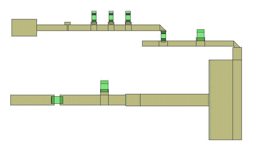
elements involved in just a simple two stage amplifier ( It fills an A3 page ),
the Voltage regulator circuit was added later in the CAD layout of the board
after it had been generated in Microwave Office
using the relevant layout tools this means that you
can see the effects of the grounding you add as you create a full PCB artwork
remembering to ADD all the relevant text to aid testing & inspection of the
completed project. Having created the schematic in the modelling package the
design is then transferred to a basic layout this only has components &
microstrip on it the ground plane and board outline together with the relevant
text to be etched on the Top copper layer are now added , this enables you to
check that any grounding alongside microstripline does not turn into "
Coplanar stripline " shold you need to extend tracks up to the edge of the
board to fit it in a standard box then these can easily be re - modelled at
this stage before committing the design to production . The
stages in reaching the completed artwork ( including the " Mirroring
" to produce a contact print ) are detailed in the modelling package but
the instructions are often buried several layers down in the help files . This
is a simple stage by stage set of instructions to enable anybody starting off
using the modelling packages to get an artwork out ready for exposing a Photo -
Sensitve PCB substrate .
The simple " Step by Step " instructions
for using Microwave Office for these projects are
listed below
Lay out your circuit using the relevant components &
symbols from the MWO library or download them from the manufacturer's sites ,if
your chosen component has to be loaded as a subcircuit using just the" S2P
" data from the manufacturer's website then there is a work around to get
the package , simply use the MWO website to find a device with the same package
as the device you have only the " S2P" for simply add this to your
drawing at schematic level as a " Floating " component then when you
go to the layout place it where you require it , this is not perfect but will
at least enable you to get an artwork with the right size component footprint ,
it will also show up correctly in the 3D visualisation .
Then add all the graphs you think you will need together
with any text, when you have your desired amplifier completed at schematic
level .
Then convert it to a layout using the relevant part of
the program , you will end up with a " Rat's Nest " of all the parts
don't forget if you have had to add a device for it's footprint to place it in
the correct location at this stage .
Now lay these out as per your circuit diagram , the
individual elements in the layout are highlighted as you move them ( if you
wish to check back to the schematic you will see them highlighted accordingly
in Green ). Then using the select all the items you wish to place , then from
the tool bar using the " Snap
Together " tool you can automatically place all the tracks
& components that are highlighted , this saves a lot of time laying out the
parts to join accurately , you may also use this tool if you modify the layout
, for instance to fit a standard sized case , don't forget to go back to the
schematic page & redo the simulation eg when you have bent a trace to fit (
eg when using " MTRACE2 " ) or you have
added the top side groundplane which is not
automatically generated by the package to enable
decoupling capacitors to be grounded you may also need to add holes to make
connections through the board to the main groundplane , the spacing of these
holes in general should be less than L/4 to ensure no stray resonant currents
build up in the top side ground plane with respect to the lower groundplane .
With the microstripline used to go to the ports of the circuit it is advisable
to allow for about 10 mm of system impedance ( 50 R ) for the legs of the edge
transition SMA connectors , don't forget to buy the right type for the
thickness & spacing to suit your board height & transmission line width
!
An
interesting point to remember when using these edge transition connectors is
that the legs that fit over the PCB are in fact protruding from the groundplane
( Body of the SMA ) and at certain frequencies these may be coupled in to the
transmission line causing problems when the are 1/4 wavelength long they become
Monopole aerials this happened on a wideband
aerial for 12 - 14 GHz !
Then add a shape for the housing you intend
using using the " Layout
editor " ( Toolbar at the bottom of the screen or drop
down menu ) to " Add
Shape " this will put a shape up coloured in as
" Error " initially .
Then by using the "
Shape Properties " command you
can change it to " Board
Outline ", then you can repeat the " Add shape
" routine to ADD the groundplane as you require
" Copper Layer
" being chosen . By returning to the schematic part of the program
you can see the effects on the circuit of adding the grounding areas changing
line lengths to fit the board outline etc , Text can be added using the text
editor on the taskbar ( The same way as you added text to you circuit &
graphs earlier ).
Then when you have your completed design laid out copy
the whole layout ( if more than one layer then check each one ) & mirror it
and place it on the page below the " Normal " layout also you are
advised to label the mirrored artwork with the relevant wording ( "
Mirrored Artwork this side to copper " ) and in the case of a multi -
layered design add a reference point " A " on ALL layers to ensure
the correct aliginment , you are now ready to export your completed layout in
to one of the CAD packages mentioned on this website , exporting it as a
" Flat DXF
" is the easiest option , this is then read in to the CAD package (
You will have to set the drawing defaults up at this stage see the
relevant webpage
) .
Then you can finally colour the relevant areas of you
layout in according to whether you require a photo positive or photo negative
artwork you will need to choose the approriate colours for all the lines in the
drawing otherwise the individual shapes drawn will be just that NOT joined up
tracks !
The Circuit design and Graph of modelled results
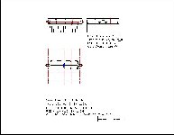
The PCB Layouts are shown in stages ,the only
difference between the artworks is the ground has been added using the Layout
editor in MWO for the second PCB layout and the
mirrored artwork has been added in the second layout.
The CAD artwork this is derived from second layout above
, the DXF exported from MWO with the normal &
mirrored layouts ready to fill to create the " Contact " print which
can also be copied in to a word document .Note you may have to select the
appropriate layer ( Top Copper ) during the exporting of the DXF as the view
includes the component outlines .
Alternative attenuators for gain setting
The Finished module

Parts Listing for the Module ( Includes all gain setting
values )
| Item |
Manufacturer |
Part No. |
Supplier |
Supplier's Part No
|
QTY |
| 78M08 |
Various |
78M08ACDT |
Farnell
|
516 - 4929 |
1 |
| GALI5 |
Minicircuits
|
GALI - 5 |
Minicircuits
|
GALI - 5+
|
1 |
| GVA84 |
Minicircuits |
GVA-84 |
Minicircuits |
GVA - 84+
|
1 |
| 1R2 " 0603
" |
Various |
|
Various
|
|
2 |
| 5R6 " 0603
" |
Various |
|
Various |
|
1 |
| 12R " 0603
" |
Various
|
|
Various
|
|
1 |
| 18R " 0603
" |
Various
|
|
Various
|
|
1 |
| 33R " 0603
" |
Various
|
|
Various
|
|
1 |
| 39R " 0603
" |
Various
|
|
Various
|
|
1 |
| 180R " 0603
" |
Various
|
|
Various
|
|
4 |
| 330R " 0603
" |
Various
|
|
Various
|
|
4 |
| 390R " 0603
" |
Various
|
|
Various
|
|
4 |
| 680R " 0603
" |
Various
|
|
Various
|
|
4 |
| 820R " 0603
" |
Various
|
|
Various
|
|
4 |
| 1K8 " 0603
" |
Various
|
|
Various
|
|
4 |
| 100pF " 0603 " |
Various
|
|
Various
|
|
6 |
| 1nF " 0603
" |
Various
|
|
Various
|
|
2 |
| 100nF " 0603
" |
Various
|
|
Various
|
|
3 |
| SMA Socket |
Various
|
|
Farnell |
105 - 6374 |
2 |
| 10nH |
Coilcraft
|
1606 - 9 - LB
|
Coilcraft
|
1606 - 9 - LB
|
2 |
| 50 x 25 x 15
case |
Perancea |
PFL - 2 - T |
Farnell
|
118 - 1374 |
2 |
Single stage Amplifier
for 3.4 - 3.8 GHz Wlan band using a GaN Fet
This module is designed to produce about +30 to +33dBm
using the NPTB0004 for driving the output stage in a Doherty amplifier using a
pair of NPT35015 GaN Fets , it uses the "Standard " GaN Fet bias
power supply module
Versatile Bias
Regulator for GaN Fets mounted on the case of the amplifier module,
although with a little effort it could be redrawn to fit on the main PCB on one
of the large ground areas ( future work ? )
Circuit of 30dBm Wlan Amplifier
Graph of Amplifier responses ( S11, S21
& S22 )
Artwork of 30dBm Wlan Amplifier
Mirrored Artwork ( Photo - negative
)
3D View of PCB ( MWO )
15 Watt Single stage Amplifier for
3.4 - 3.8 GHz Wlan band using a NPT35015 GaN Fet
When you design your circuit using a modelling package
you should be aware of the needs of the physical implementation of your design
so that to design this amplifier the starting point was the manufacturer's test
circuit for the device ( LINK )
this technique applies to ALL circuit modelling packages but as I'm used to
using Microwave office I'll give more detailed instructions for this package (
I've also tried it out on the free " Designer SV " package at home )
this is the design for a 15 - 20 Watt broadband amplifier using the GaN fets
available from Nitronex together with it's 2
Watt driver the 10 Watt amplifier uses the NPTB35015 & the Driver uses the
NPTB0004B the circuits are designed to be wide band with as flat a frequency
response as practicable so the use of " Tunable components " is
avoided ,the various elements are chosen from the library of the modelling
package or the individual manufacturer's websites & inserted as
sub-circuits using the software for the components which are not contained in
the relevant libraries , Micro-strip elements & board parameters are
usually in the manufacturer's libraries in the package ,but you often have to
use " Online " libraries for upto date data for individual components
.Some of the modelling packages have an in built optimisation tool to tune the
design from your layout , whilst this may save time for some users it must be
noted that this is NOT " Intelligent " it will only work within the
parameters that you the designer specifies ( You can easily put
one track down the middle of another ) .The way the lengths & widths of the
individual elements are written will enable the software to do the optimisation
but the designer will need to specify the ALL the relevant limits , so by
carefully adding in ALL the elements needed to replicate the layout of the
manufacturer's test board it is possible to reproduce it , however there are
some " Tricks " to laying out the board such that the assembly can be
done with minimum recourse to moving parts to obtain the required performance ,
for instance it is easy to model a shunt capacitor from a transmission line to
earth but actually placing it to sub millimeter accuracy by HAND is another
problem , so why not use the modelling software to help you , by using a
microwave junction ( Tee or Cross ) you can add a short < 0.5mm track equal
to the width of the shunt element , this will produce a definite location on
the transmission line to locate it , ( the beauty of this is the software also
knows it's here ! ) so you should get the results you expect . Also as you
design the bias tee's ( Gate & Drain ) you should ensure that there are
pads of fixed width equal to the transistors connection to ensure that the
optimisation tool does not produce tracks that are too narrow to support the
device or put them up the middle of the transmission line ( you have to specify
the line lengths correctly just look at the circuits below to see how to do it
) the components in the bias tee's will require spacing to permit the soldering
of individual components so tracks of a minimum length should be included in
the design , again it is you the designer who knows the minimum spacing for
your soldering skills . If you do not have the footprint / layout from the
modelling package's library ,there is a work around whereby you can include a
device with the footprint of your chosen device somewhere on the circuit ( BUT
NOT connected to it ) this is to enable you to place the tracks at the correct
spacing to enable the final layout to be produced before exporting it to
generate the artwork , you could always learn how to create component layouts
in an appropriate CAD program then import them as the program designer's intend
you to ( but then that's another story !) . The circuit parts shown below have
all the relevant information set in their parameters each limit is explained
for each circuit together with the final layout of the completed board , this
will just need mirroring in the layout editor to produce the contact print as
most CAD packages do not mirror the text you have included on your design put
it in the layout in your modelling package !
The Amplifier Input & Gate bias circuit
The layout of the input circuit
The circuit as initially modelled , before the added
copper pads for the top groundplane which when added are shown in a different
colour to the modelled microstripline , these will of course all end up the
same colour when you do the CAD work , to complete the artwork according to
whether it's photo - Positive or Negative artwork required .
The Amplifier output Circuit & Drain supply
The layout of the output circuit
The combined circuits are shown below ( note this was
before the revised circuits for the bias networks were used to ease the placing
of shunt components )
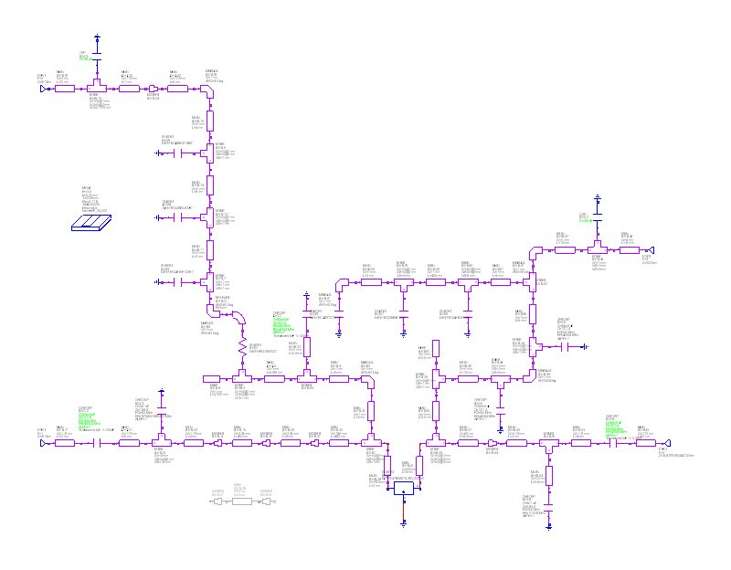
The Completed layout showing all the relevant features
combined this is before any ( optional ) text has been added to identify the
connections or " name " the board , this being done by removing the
large areas of groundplane and replacing them with smaller areas around the
text along with any fixing holes neccesary to secure the board to it's housing
/ heatsink .
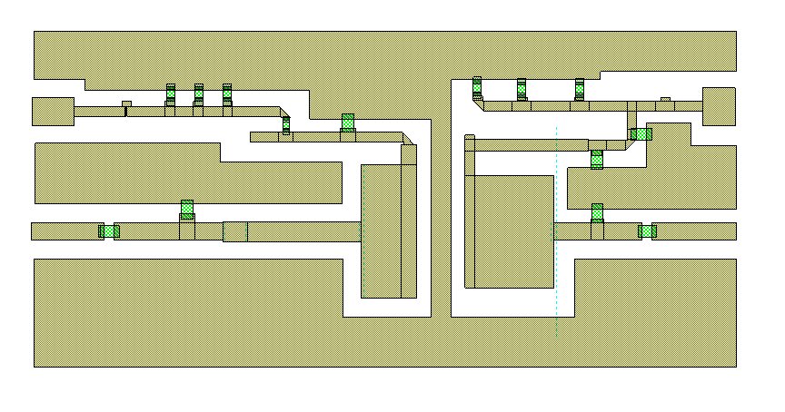
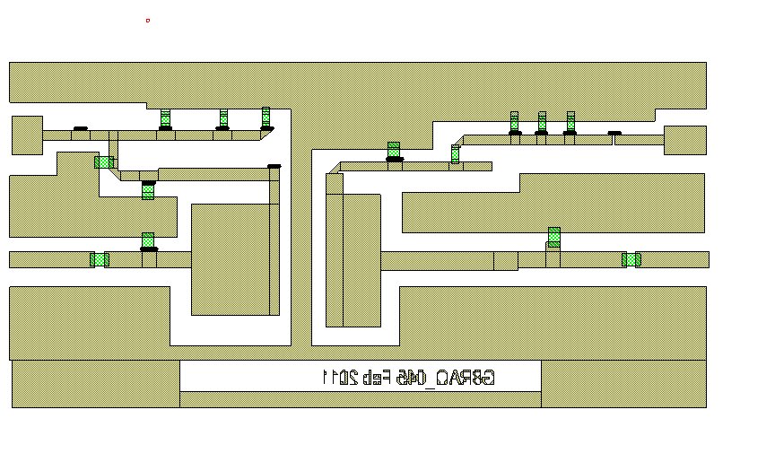
The mirrored artwork is now ready to print out for a
" Contact " printed PCB when exported via you CAD package ( Currently
I use either
Quickcad
or it's replacement
Autosketch
)

The final " Mirrored " artwork ( with text )
from Microwave Office prior to exporting to the CAD package
Back to RF Design For Students
This page last updated 16th May 2013
