Basic Design
Notes for Printed Circuit Boards For RF Circuits
Before creating your PCB you will need to choose
ALL the components needed to fit on to your pcb , remember if you
intend to use the edge transition coaxial connectors that they have different
sizes of leg spacing between the center conductor & the coax outer ( legs )
this will influence the choice of substrate to be used ,in order to design to
avoid shorting out the connector / coaxial cable because you've chosen the
wrong parameters ( Dk & thickness )! I will have fully worked examples of
High Pass Filter & RF Low Noise Amplifiers on my Amateur Radio projects
pages shortly .
If you are creating a multi layer PCB it is advisable to
put alignment & reference marks on each layer so that correct alignment of
the layers can be achieved , the use of a " board outline " option
can add an unwanted single turn loop around your circuit (
you've just added a single turn transformer secondary
), if your design requires more than two layers then to assemble the
composite you will have to think more about the mechanics of this assembly.
Accurately placed pads that can be drilled in each PCB for non metallic
fasteners ( eg Nylon Screws ) to provide the alignment is a relatively easy
process ,this also means that with the correct spacing of the screws you can
ensure that the layers are spaced as per your design and not have any air gaps
to change the dielectric layer in the structure as it is flexed during testing
/ handling . Obviously the size of pad should be less than the thread diameter
of the fastener to be used so that ALL of the metal can be
removed by the drilling out otherwise the metal pad will affect the designed
radiation pattern in the case of an aerial . For a fully detailed project using
Microwave Office with all the stages for
design & fabrication follow this link ( Dual MMIC amplifier)
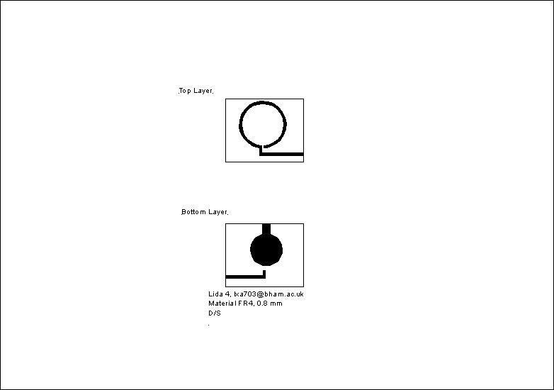
Having created your PCB artwork(s) using the appropriate
software , it is neccesary to printout the artwork(s) ready to produce the pcb
, the process used is to make a contact print for each layer of the PCB ,
remember the " Top " layer of a double sided PCB will need to be
mirrored in order to maintain the printed layer in contact with the photo -
sensitive layer on the PCB conductor. Each layer of artwork should be labelled
with the relevant contact details , substrate material & layer you should
also incorporate cutting symbols at the corners of the PCB as the fine lines
created by the software for board outlines often get etched away or need to be
removed for electrical reasons eg on an aerial design , the easiest way is to
use the " + " symbol at the corners of your pcb . If the PCB is to be
single sided with a ground plane then again this information should be included
on the printout eg " D/S with groundplane " although the ground plane
may not be needed to be printed unless you have clearance holes in it
. With microstriplines close to the edge of the pcb
you have designed if it is going to be cased then you should allow at least 3
track widths from the edge of the microstrip to avoid interaction between the
line & the case ( A Coplanar wave guide could be formed otherwise ) unless
you are using " Shunt " elements ( eg Capacitors for matching ) as
part of your design.
When designing with either Microwave Office , ADS or CST Microwave you should
be aware of the following requirements needed to create an artwork .
If you are using " Pre Coated FR4 " as the PCB
material you will need to create a " Photo Positive " master however
if you intend to use " Duroid " or a similar uncoated substrate then
the process to coat this material is different , in that a " Photo
Negative " artwork is required and you will need to ensure you design your
layout accordingly .In industry your artwork would normally be exported to a
draughtsman to further process ,Microwave
Office 2006 has a DXF output
option , however Microwave
Office 2007 or later also has a Gerber Output function in
it to produce artworks using a laser plotter . CST
Microwave currently only supports outputs in DXF for artworks (
the BMP option is only 96 DPI good enough for putting your design in to a
document but NOT artwork quality !) ADS currently only supports
outputs in DXF.
Should your pcb need to be mounted in a custom housing the option
of " Export in DXF " from your chosen PCB package should be used to
enable you to design a housing using one of the many CAD packages available
.
The currently
available software for POST GRADUATES &
RESEARCH STAFF from Comms Group is Quickcad
& Autosketch to convert the files
from DXF format to generate the artwork then save it as a .CAD / DWG or
equivalent format .
For
ALL Taught Course Students there is
a choice of a work around using the packages currently available in the lab
N218 using Autosketch
to import the DXF then save it
(SKF) then open it using to
fill the outlines etc OR you can use Autodesk's " AUTOCAD 2010 " using a downloadable copy
available to students by contacting Autodesk directly but this cannot be used
on EECE PC's .
Please follow one
of the links for detailed instructions .
For " Taught
Course Students " If you have any questions about the
software you are using to create your PCB then you should ask your SUPERVISOR first ,not the support staff as they
may not use it on a regular basis .
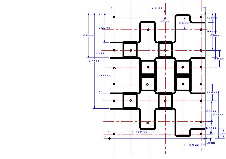
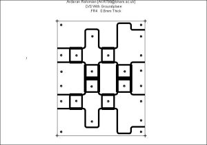
A typical Student's artwork
Here is a more complicated design created using
Microwave Office for a " Butler Matrix " the fine lines for the board
outline are often etched away during the production of the board so the use of
" + " symbol to define the corners is advisable , also note
the fixing pads for the mounting screws as the completed board is to be housed
in a metal enclosure these pads are SMALLER in diameter than the screw thread
so that when they are drilled out there will be no metal left to affect the
design ( IF you use NYLON screws to secure the board ) or you can use metal
screws with a possible change in performance ( You could always model the screw
! )
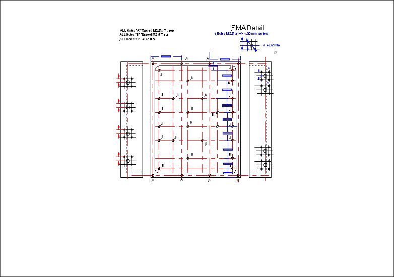
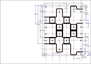
The same PCB artwork with the centre lines used to lay
out the pads accurately , this drawing is used to construct the housing around
the PCB
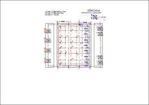
The drawing for housing the PCB.
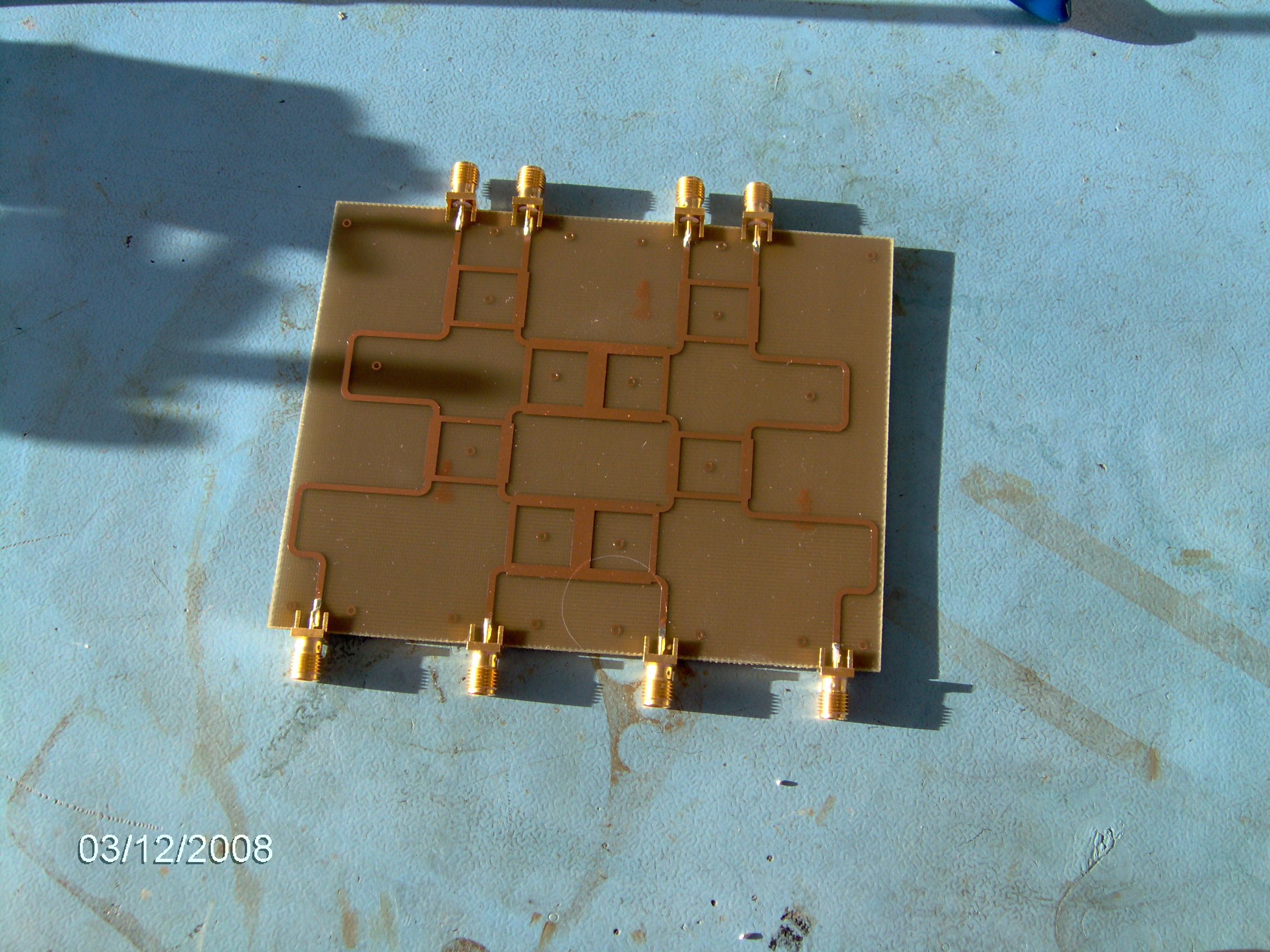
The completed PCB ready to test before fitting in the
housing .

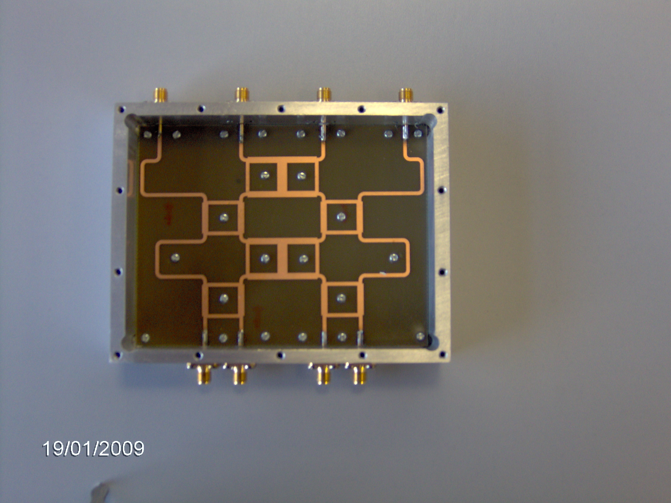
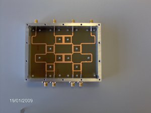
The finished article , the PCB in it's
housing
Having finally arrived at your completed
artwork it is advisable to Email the person responsible for making your PCBs
both of the quantity and any specific delivery date , it is also advisable to
include your contact details on the artwork ( University Email address / phone
number ). But , please bear in mind , there is a
typical lead time of up to 5 working
days between printing out your artwork together with handing in
the unetched substrate & receiving an etched PCB .This is because if other
members of staff have to cover the " normal " person , should this be
the case then information can then be forwarded accordingly , also stick on
" Post - it's " have a habit of blowing away or otherwise getting
lost , so please use Email!
For ALL " Taught Course " ( BEng , MEng &
MSc ) students this is Robert Davies R.K.Davies@bham.ac.uk he may then pass you on to one of
his technicians .
For MRes , MPhil & PhD in Comms group this is Alan
Yates A.C.Yates@bham.ac.uk
Back to RF Design For Students
This page last updated 15th Jul
2015